Global Nanopatterning Market Analysis and Future Growth Outlook to 2031
Nanopatterning is an advanced fabrication technique that enables the creation of structures at the nanometer scale with high precision and repeatability. It is essential for developing next-generation electronics, biomedical devices, and high-performance materials. By controlling surface patterns at the nanoscale, nanopatterning enhances functionality, efficiency, and customization across various industries.
The Nanopatterning Market is experiencing rapid growth, driven by increasing demand for miniaturized electronics, innovative medical devices, and eco-friendly manufacturing processes. Businesses are leveraging advancements in lithography techniques, including nanoimprint, photon-based, and electron beam lithography, to deliver high-precision products. Rising awareness about the benefits of nanoscale structuring is also motivating end users to adopt nanopatterning technologies in both research and commercial applications.
Driving Factors
The Nanopatterning market growth is fueled by the need for ultra-compact and high-performance electronic devices. As consumer electronics, sensors, and semiconductor components become smaller and more powerful, nanopatterning provides the precision required for these advanced designs. In the healthcare sector, nanopatterning enables the creation of personalized medical devices, improved diagnostic tools, and targeted drug delivery systems, further boosting market adoption.
Technological innovations in lithography methods are also driving growth. Advancements in nanoimprint and photon-based techniques allow faster production with higher accuracy, while electron beam lithography offers exceptional resolution for complex structures. Additionally, the push for sustainable manufacturing practices using eco-friendly materials has created new opportunities for nanopatterning applications in clean energy and green technologies.
Market Trends
The Nanopatterning market is witnessing a shift toward personalized and application-specific nanopatterning solutions. Customized patterns are increasingly being used to enhance the performance of medical devices, optimize electronic circuits, and develop innovative organic devices. There is also a growing emphasis on integrating nanopatterning with digital fabrication methods and automation, improving scalability and reducing production costs.
Sustainable nanopatterning is emerging as a key trend. Companies are exploring biodegradable and environmentally safe materials, as well as energy-efficient fabrication processes, aligning with global initiatives for eco-friendly manufacturing. Another trend is the convergence of nanopatterning with emerging technologies like flexible electronics, wearable devices, and biosensors, expanding its applications across diverse industries.
Download Sample PDF: https://www.theinsightpartners.com/sample/TIPRE00009279
Growth Opportunities
Significant opportunities exist in the development of next-generation medical devices with tailored functionalities. Nanopatterning can enhance device sensitivity, improve drug delivery mechanisms, and enable non-invasive diagnostic tools. In the electronics sector, precision nanopatterning can drive the production of smaller, faster, and more energy-efficient chips and sensors, supporting innovation in consumer electronics, IoT devices, and autonomous systems.
Additionally, the renewable energy sector offers potential for nanopatterning applications, such as enhancing the efficiency of solar cells and energy storage devices. Partnerships between technology developers and end users can accelerate adoption, while continued R&D in materials and lithography techniques can expand the versatility and accessibility of nanopatterning solutions.
Key Players
- Toppan Photomasks
- AMO GmbH
- OraSure Technology
- Micro Resist Technology GmbH
- Nanonex Corporation
- NIL Technology ApS
- Nano Terra
- Akers Biosciences Inc.
These companies focus on technological innovation, strategic collaborations, and expanding their geographic presence to strengthen their market positions and address growing demand.
Future Outlook
The future of the Nanopatterning Market is promising, with sustained growth expected as industries increasingly demand high-precision nanoscale solutions. Expansion into emerging markets, integration with digital fabrication, and continued innovation in lithography techniques are expected to drive the market forward. As applications broaden across electronics, healthcare, and renewable energy, nanopatterning is likely to play a pivotal role in shaping the next generation of advanced devices and sustainable technologies.
FAQs
1. What is driving the growth of the Nanopatterning Market?
Growth is driven by the demand for miniaturized electronics, advanced medical devices, and sustainable manufacturing processes.
2. Which industries are adopting nanopatterning technologies the most?
Key industries include electronics, healthcare, renewable energy, and consumer devices, where high-precision nanoscale patterns enhance performance.
3. What are the future opportunities in the Nanopatterning Market?
Opportunities lie in personalized medical devices, flexible electronics, renewable energy solutions, and integration with digital fabrication and automation.
Related Report
Gene Therapy CDMO Market – Contract Development & Manufacturing Analysis
Категории
Больше
The global pruritus drug market size was valued at USD 7.99 billion in 2024 and is expected to reach USD 11.90 billion by 2032, at a CAGR of 5.10% during the forecast period. The global business landscape is undergoing a transformation, with industries increasingly leaning on deep research and actionable insights to make strategic decisions. One segment seeing...
Technological innovations are driving the growth of the Japan Healthcare Cold Chain Monitoring Market. Real-time monitoring devices, resistance temperature detectors, and conventional temperature loggers are increasingly used to track temperature and humidity during the transportation and storage of vaccines and biologics. Integration with cloud-based software allows for real-time reporting,...

Market Trends Shaping Executive Summary Europe Psychedelic Drugs Market Market Size and Share Europe psychedelic drugs market size was valued at USD 337.40 million in 2024 and is projected to reach USD 878.09 million by 2032, with a CAGR of 12.7% during the forecast period of 2025 to 2032. An excellent Europe Psychedelic Drugs Market Market report gives out all-encompassing study...
The handheld metal laser welder has transformed modern welding practices by offering unmatched precision, speed, and efficiency. Unlike traditional welding methods, this advanced technology uses a focused laser beam to join metal components seamlessly. Whether in manufacturing, repair, or fabrication, this innovative solution provides exceptional results with minimal effort. At Laser China, the...

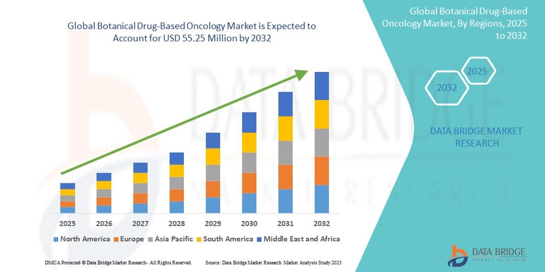
"Executive Summary Botanical Drug-Based Oncology Market Opportunities by Size and Share CAGR Value The global botanical drug-based oncology market size was valued at USD 28.12 million in 2024 and is expected to reach USD 55.25 million by 2032, at a CAGR of 8.81% during the forecast period Botanical Drug-Based Oncology Market research report is a...